

 Global
  United States
A Brief on Electronic Product Design
Electronics systems and gadgets have become an integral part due to the surge in innovation and technological advancements, including 5th generation (5G) wireless networking, augmented reality (AR), virtual reality (VR), artificial intelligence (AI), quantum computing, miniaturization of semiconductors, Internet of Things (IoT), machine learning (ML), biometric authentication, and more. Consumer electronics like smartphones, home appliances, televisions, laptops, tablets, cameras, LEDs, adapters, wearables, gaming consoles, and others represent a major portion of customer spending given their daily usage.
Electronic product design is a process that includes customer requirement gathering, extensive market research, component selection, product creation, feature enhancements, product lifecycle governance, and post-market support. Managing all these aspects in consumer electronic product development while meeting project deadlines can result in businesses trying to outsource components and processes to vendors, rendering timely coordination and costly redesigns as constraints.
Reliable, scalable, and compliant (FCC, CE, ISO, RoHS, WEEE, FDA, or ACME) electronics design requires critical discipline that transforms ideas into market-ready products via a well-structured design approach offered by electronics manufacturing services. This may include developing a Minimum Viable Product (MVP), product prototyping, firmware development services, Printed Circuit Board (PCB) design, thermal optimization, power management, etc., to attain product success with minimal time to market.
The Indian market for consumer electronics products is estimated to be around ₹9,768 crores as of 2025 and is expected to surge and reach an approximate value of ₹124,429 crores by 2035, increasing at a CAGR of 9.6% during this forecast period. The rise in electronics development services is majorly due to expansion in the housing sector, growing governmental funds, urbanization, and investments.
Source: Grand View Research
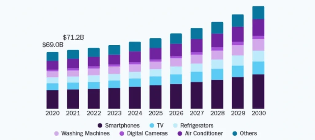
Growing market size of consumer electronics products during the forecast period 2020 to 2030
Major Challenges in Electronic Product Development
While developing a new product, if the process, strategy enclosure, or the type of electronics to be developed is considerably novel, it could result in unnecessary expenses. Here is a list of some of the common technical pitfalls that can lead to expense inflation and product development failure.
Electrostatic Discharge
There can be instances of a momentary surge of electric current flow from one charged source to another when they are kept close enough. Electrostatic discharge (ESD) threats can occur between the user and the device or charged cables. ESD needs to be grounded as they remain in the device, moving air, and installation sites for longer durations, especially in dry conditions, for example, electric muscle stimulation device.
As circuit boards are increasingly susceptible to such discharges due to various soldered points, it can cause internal damage to the device, reduce its lifespan, and lead to premature failure. A high-fidelity wave simulation tool called the full-wave solver is required to model ESD threats in product designs. Often coupling to cables that are involved with sub-millimeter filaments in braids can pose modeling challenges.
Electromagnetic Emissions
These types of noises and emissions are generated unintentionally from electronic devices and can interfere with the working of other devices. They may be caused by compact circuit designing, deploying multiple devices at the same frequency, and antennas. Radiated emissions cause data loss, safety risks, inaccurate readings, and even device malfunctions, which need to be resolved during consumer electronics product design.
One can minimize these emissions in cables and circuits by utilizing EMI filtering, bonding, proper wiring, cabling, grounding, and shielding. The limits of these emissions range across many frequencies, thus leading to testing failures in the early developmental stages. The frequency should be rendered small for predicting potential peaks during simulation, while modeling the entire enclosure using legacy methods is costly and complex.
Electromagnetic Interference
The transmission line or circuit, when placed in adjacent positions with other pieces or components, can interfere with their functioning by generating signals. All electronic systems like integrated circuits (ICs), PCBs, and communication cables can produce electromagnetic (EM) fields that overlap, causing crosstalk. This results in degraded signal quality and unintended coupling between radio frequency (RF), analog, and digital blocks.
One can mitigate this complex issue by reducing the width of traces, using differential signals and ground planes, and keeping adjacent layer traces as perpendicular as possible. Ferrous chokes, foams, absorbing tapes, and tiles can be used to reduce EM interference. It is necessary to state their importance in the early stages, as these advanced materials can be frequency dependent, expensive, and stringent standards during the design.
Circuit Designing
The circuit board developed through circuit board and manufacturing services, is made of laminate like epoxy, fiberglass, and layers of circuits comprised of copper, which connect different electronic components within consumer electronics products. Excessive components can lead to an increased bill of materials (BOM), thus necessitating a reduced number of layers in the PCB stack. Moreover, EM interference that causes incompatible signals and failure of board functions is generated due to flaws in the designing of PCB coils, circuits, and traces.
PCB layout recommendations and samples can be useful for switching regulators, as they are more sensitive than linear ones and can make the circuit unstable. Designers can add physical shielding, trace layout, PCB grounding, and component arrangement to mitigate these problems. They need to keep unpredictable high-frequency noises in mind that travel across the boards. Trace width is of importance, especially when they carry more than 500 milliamps, as narrow ones can overheat and cause failure.
Thickness depends on temperature limits and whether the trace is on the inner or outer layer, where the latter can withstand more current per width and heat dissipation. It is usually advised to follow best practices, design rules, injunctions, and high-fidelity PCB modeling to prevent such issues. At times, the CAD tool libraries do not include new parts, which lead to newer PCB landing patterns and subsequent errors like unsolderable areas. PCB can be printed at 1:1 scale, and the components can be placed physically to avoid reworks.
DFM Failure
To tackle major challenges in product development from the design phase, one needs to consider affordability, reliability, repeatability, and the scaling scope of the design for manufacturing (DFM), as small changes in later stages can pose issues. The overall cost estimate, including those for production and manufacturing, must not be procrastinated, as it leads to a lack of customizations and high sale prices.
Redesigning the same could extend the time-to-market and increase expenses, thus ballpark costs should be finalized prior to design or medical prototype development. Brainstorming sessions and external feedback before prototyping, representing independent design engineering views, can be helpful to reduce iterations and related costs.
Others
Other design challenges include incorrect design of wireless circuits in hardware products developed by hardware development services that feature RF, Long Range (LoRa), Wireless Fidelity (Wi-Fi), and Bluetooth connectivity. Main considerations are related to antenna tuning, impedance matching, transmission lines, width, shape, position of trace, etc., for accurate signal flows. Matching circuits can be useful, such as a pi-network consisting of inductors and capacitors in the case of transmission lines connecting RF to fine-tune antenna impedance. Pre-FCC-certified wireless modules can also reduce costs and simplify development.
Chips receive stable voltage through well-placed decoupling capacitors, such that each cap is placed close to the power pin so that the power trace hits the cap before it arrives at the chip. For transient response, better stability, and preventing oscillations in the feedback loop, the output capacitor needs to be placed near to a voltage regulator’s output pin, wherever applicable.
At times, the injection molding developed through electronics product design services may not be compatible with the enclosure design, which can be resolved by using 3D printing for enclosure prototyping. Iterations through this method can make mass production using high-pressure injection molding possible, given design rules for ejection paths, wall thickness, and draft angles are followed strictly, for example, in a wearable technology design.
Traces are routed between specific layers over the board by using buried and blind vias, which are useful for compact designs but arduous to manufacture. This doubles the prototype cost and reduces the possibility of creating boards as per the layer stack. Through vias are less costly, reliable, and simpler in comparison and thus are commonly used in prototyping.
E-Waste & Supply Chain Regulations
With increased iterations, e-waste generation can increase profoundly, ending up in landfills, waste streams, and households, unless collected and recycled. In some countries, manufacturers face compliance issues (ESPR, EPR, Anti-Waste, and Circular Economy Law) where they are subjected to offering repair beyond the warranty period, providing spare components up to a decade, displaying a repairability score (for smartphones on the A to E scale), and issuing a Digital Product Passport to electronics. They face direct legal exposure if their designs include non-replaceable batteries, proprietary and obsolete parts, and legacy software that slows down devices, especially in medical equipment engineering.
Challenges in the Device-as-a-Service (DaaS) model and supply chain, such as the pandemic and increased tariffs for Dynamic Random Access Memory (DRAM), not only cause shortages in components and semiconductor-based material but also geopolitical instability and reshaping of cost structures. Apart from these market trends in electronics product design and development, upgrade cycles, on-device AI replacement, margin pressure, incremental hardware improvements, aggressive discounts, market saturation, K-shaped economies, and greenwashing risks are being observed globally as customers own more than one device and know the products well.
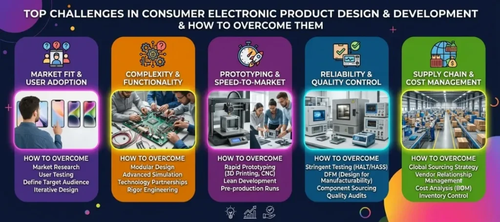
Various challenges in consumer electronics product design and steps to overcome
Best Practices for Electronic Product Development
Businesses need to focus on reliability engineering, design for testing (DFT), DFM, and cost optimization to streamline product development and improve quality. This section explores certain factors to be kept in mind for developing compliant, cost-efficient, and scalable products.
Thermal Management
Miniaturization trends increase component density, noise monitoring, signal interference, and heat generation that can impact reliability, functioning, integrity, and performance. Repair of minuscule components and iterations requires heavy investments and advanced designing and manufacturing techniques. Shrinking power supply is another issue to be dealt with without compromising safety and capacity, such as in a FPGA design. A multi-faceted approach that includes high-density interconnect (HDI) PCB designs with finer traces and microvias allow signal integrity even incompact placement.
Passive components and multiple dies can be integrated into a single package to minimize footprint, also known as the 3D integration and System-in-Package (SiP) technique. Thermal analysis and simulation tools can be used to highlight hotspots during the design phase and manage optimal temperatures through adept implementation of heat pipes, thermal vias, and heat sink designs. With RF and high-speed digital design expertise, low-profile components can be selected to reduce signal lengths and EM interference.
Power Efficiency
Although efficient power utilization is a major design consideration in electronics product design services, battery-powered feature-rich devices cannot run adeptly on low power. Balancing power consumption, performance, and longer battery life in low-power embedded devices, portable, and IoT-based electronics becomes difficult unless backed by IoT consulting services. As these devices comprise high-performance peripherals, software and firmware overhead, frequent processor wake ups, and inefficient code, they pose a power drain and penalty. Even in a low-power state or deep-sleep mode, devices may face current leakage that can cause the battery to drain.
Moreover, power conversion from source to components and their consumption needs to be efficient. A holistic approach towards system-level optimization, firmware development, and hardware design needs to be employed. This includes clock gating, dynamic voltage and frequency scaling (DVFS), power gating, and other low-power design techniques. The system should be enabled with intelligent power management algorithms such that it spends maximum time in a deep sleep state. The processor may remain in a high-power state due to continuous polling, which needs to be minimized through event-driven architectures, while computational load can be reduced through efficient and optimized code.
Edge AI
The data flow over the cloud for processing has increased over the years due to a surge in IoT device management, resulting in low bandwidth, privacy issues, and latency. Although decision-making and data processing can be done at the device level through edge AI deployment, it involves certain hardware constraints from the perspective of energy, memory, and processing power.
AI/ML models need to be optimized, reduced in terms of size, power consumption, and computational needs when rolled out on battery-operated edge devices by any product design services company. Also, data across sensitive applications needs to be managed and secured at the edge. To tackle these issues, one can utilize neural processing units (NPUs), GPUs, and CPUs, forming a heterogeneous computing architecture for system-on-chips (SoCs).
ML models can be optimized into efficient and lightweight ones in this scenario by using quantization and pruning. Here, the former involves reducing the precision of model weights, whereas the latter deals with removing model parameters that are not required. AI can be run on resource-constrained appliances with the aid of TensorFlow Lite, Edge Impulse, uTensor, microTVM, STM32Cube.AI, emlearn, Kneron SDK, CMSIS NN, and other TinyML frameworks for microcontrollers.
Wireless Technology
Electronic products connect to the internet, cloud, and IoT devices via Bluetooth Low Energy (BLE), Wi-Fi, Long Range Wide Area Network (LoRaWAN), cellular connectivity, and other communication protocols. Selection of the apt one as per the data rate, power, and range is required to tackle such challenges in product development. Developing an effective antenna designed and integrated for a compact wireless device that runs without any effect from coexistence and interference from other devices can be challenging.
To tackle these issues, especially in the case of medical device design and development, expertise in wireless protocols, antenna tuning, and antenna simulation tools are needed. Mitigation strategies for interference and coexistence can be adopted, such as adaptive frequency hopping algorithms, shielded components, and frequency planning. Device battery life can be extended by using low-power connectivity protocols like BLE, Zigbee, and LoRa to reduce power consumption.
Regulatory Compliance
Define customer requirements and use cases, identify target audiences; highlight pain points, expectations, technical literacy, and develop a product requirements document (PRD) prior to circuit designing and coding. Make sure the design complies with certifications, international and regional regulations, especially in the case of medical device contract manufacturing, such as Bureau of Indian Standards (BIS), Compulsory Registration Scheme (CRS), Electromagnetic Compatibility (EMC), Telecommunication Engineering Centre (TEC/MTCTE), Wireless Planning and Coordination Wing (WPC), Equipment Type Approval (ETA), E-Waste Management Rules (2022), Legal Metrology Act, etc.
With the aid of IoT development services, one can select the right components, modules, sensors, and microcontrollers while prioritizing processing, performance, response time, functionality, battery life, and data-handling capabilities of the electronic product or IoT-based or portable device under intended conditions in real-time. Minimize per-unit costs, time-to-market, and sourcing issues by using standard components, tools for designing mechanical components, and aligning the design with the manufacturer’s capabilities.
Medical device testing procedures and firmware structure should be documented and retained for audits, debugging, future iterations, and compliance standards to avoid market rejection and legal issues. Utilize robust enclosures that can protect the circuit against compact and real-world environment impacts, moisture, and dust. Validate reliability and durability with vibration, drop, and temperature cycling tests, and enhance firmware upgradability by supporting updates that prevent firmware tampering.
KritiKal: Enabling Your Design Efficiency Imperative
KritiKal Solutions assists you in deploying a multi-faceted approach for navigating the maze of complex electronics product design and development through its advanced techniques and deep expertise. Businesses can overcome challenges related to miniaturized embedded system development and material science with us as their partners. We stand at the forefront of intelligent and autonomous edge AI applications, including driver monitoring systems and predictive maintenance in various sectors.
We avoid production risks, low-quality and non-standard components; plan thermal management and DFM; and estimate battery life and power consumption to prevent overheating. With our simulation solutions, prototyping services, and design-to-validation workflow support, consumer electronics providers can enable first-pass EMC compliance.
They can reduce development and EMI risks, testing risks, and redesigns through our automatic predictions for ESD arc attachment, induced voltages, co-simulation support for braided shields, thin conductors, cables, and mitigation measures. Businesses can leverage our agile methodologies to solve the complexity of electronic designs, growing software interconnection, communication gaps, siloed processes, and lack of requirements traceability.
We offer development and analysis of PCBs; cable coupling; enclosure efficiency; ESD using a full-wave time-domain solver; advanced thin-material modeling; PCB import from HFSS, Slwave; simulations for wide-band emission; automatic comparison for compliance limits; and frequency-dependent material characterization.
With decades of engineering experience as a product design services company, we offer expertise across development lifecycles and complex project management through proven approaches, end-to-end product design services for hardware, firmware, cloud, software, and mobile app development linked to devices; quality checks; in-house designed SoMs; and tolerance analysis using tools like CETOL 6σ, EZtol, and GD&T design fundamentals.
We understand that DaaS and circular product designing are reshaping this sector by extending product life through refurbishment, generating recurring revenue, reducing e-waste, manufacturing costs, improving sustainability, operational, and energy efficiency. Trends are shaped towards subscription models to provide predictable ROI, supply chain resilience, and minimize dependency on new inventory.
Our hardware design practices emphasize AI integration, accelerated innovation, modularity, repairability, sustainability, and recyclability through balanced performance, compliance, low costs, risks, and delivery of future-ready products. Please get in touch with us at sales@kritikalsolutions.com to know more about our embedded products, platforms, services, and realize your business requirements.

ditya Kumar currently works as a Senior Hardware Design Engineer at KritiKal Solutions. He is proficiently skilled in embedded C, UART, CAN, LIN, SPI, I2C, GPIO, USB, PWM, TIMER, easyGUI, FreeRTOS, and more. With his ability to work efficiently in teams and extensive experience in hardware design and development, he has assisted KritiKal in delivering various projects to some major clients.