


 Global
  United States
What is Surface Mount Technology?
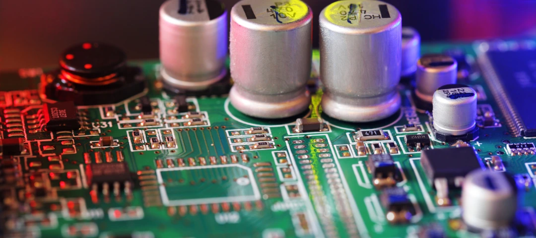
The electronics industry is inclined towards the design and development of electrical devices that function faster for longer durations and are smaller in size for increased portability. This is why the demand for surface mount technology (SMT) or planar mounting is on the rise, as it involves assembling and soldering electronic components directly onto the surface of a printed circuit board (PCB) through industrial and product design services. This technique had replaced traditional through-hole technology (THT) for miniaturized, efficient, accurate, cheaper, denser, and more compact solution development.
Electrical connections are defined by cleaning techniques, minimal leads, solder paste application, and wave or reflow soldering of these components placed or mounted through SMT since the 1960s when they were first adopted by IBM hardware development services. THT can develop larger PCBs, while SMT offers more economical options, production and labor cost-wise, as more electrical components are densely packed on the PCB to ensure greater performance. SMT is used widely across medtech, aerospace, consumer electronics, and other industries. The current global market for surface mount technology across devices and equipment is estimated to be around US $5.27 billion as of 2022 and is expected to surge and reach an approximate value of US $8.22 billion by 2030, increasing at a CAGR of 5.8% during this forecast period given the rising importance of consumer electronic product development. Let us now go through the importance, features, types, advantages, and use cases of this technology further in this blog.

Source: Roots Analysis
Growing market size of surface mount process during the forecast period 2019 to 2035
What is Surface Mount Device?
Surface Mount Devices
These are basically the electronic components that are designed and developed to be mounted directly on the surface of PCBs by electronics manufacturing services. Unlike THT, they need not have long metal leads or wires passing through the holes in the board. As these components sit on top of the PCB, their terminals are directly soldered to the pads of the surface. One may ask what are surface mount components and why embedded technology providers utilize them. These are devices or electronic components that are specifically designed to be mounted directly onto the surface of the PCB.
A few examples include surface-mount resistors, capacitors (MLCC), diodes, LEDs (3528 and 5050), transistors, integrated circuits within chips (ICs like ATmega328P and LM358), voltage regulators, inductors, connectors, etc. For instance, a surface mount device (SMD) resistor is much smaller than the traditional resistor, as the metal ends are connected through soldering mechanically and electrically.
Type of Surface Mount Device
- Basic: The components are assembled on both sides of the PCB, making it easy to use, as they are mounted without the use of any special types of tools.
- Advanced: It is seen in innovative gadgets where the components are mounted on the primary side of the board using both THT and SMT assembly types but only using SMT on the other side. This is useful for applications that require additional components on a single-sided board for higher electrical efficiency.
- Versatile: In this case, the primary side showcases the THT assembly type, whereas the components and reflow soldering are done on both sides of the board.
Benefits
The use of such devices allows manufacturers and indigenous technology services to produce lighter, smaller circuit boards and add a greater number of components to the PCB as compared to THT. The assembly can be easily automated using pick-and-place machines, which also makes the production process faster and cheaper. High-speed circuits can be established through shorter electrical connections as the components are soldered to copper pads.
Furthermore, automated soldering and assembly techniques (functioning on Gerber and CAD XY files) are impacting the manufacturing execution system (MES) that develop electronic devices. SMT negates the need for drilling holes in the board, as the PCB surface and the components are directly attached. This reduces costs related to IT solutions for manufacturing and time while improving electrical yield, as direct mounting minimizes shortened signal routes and parasitic effects.
Measurement
Certain standard or predefined dimensional identifiers are used to easily measure and categorize SMDs, such as 1812 (0.18 x 0.12″), 1206, 0805, 0603, 0201, 0402, 01005, and 008004. Smaller resistors and capacitors (Ceramic and Tantalum) are passive SMDs that utilize these codes, while the orientation of ICs and transistors (BC847 and 2N7002) is determined by package styles. For instance, a transistor has three pins that are base, collector, and emitter, and the physical package showcases the position of each of these pins as well as how to orient the transistor on the PCB. Connectors in SMT, like USB ports and HDMI connectors, are designed to save space as compared to the bulky ones used in THT.
An example would be a TO-92 through-hole transistor package with a specific pin order, location, or orientation determined by the package shape, drawing, pinout, and datasheet, while other examples are TO-220, SOT-23, and SOIC. These measurements are important to ensure that all surface mount electronic components establish stable connections, functions, deliver maximum performance, and fit accurately on the PCB electronic assembly. Similarly, IC packages can be categorized into the following types as per their functions and complexity, where QFN and BGA are the most common types of IC packaging.
- Dual In-Line Package: DIP has two rows of pins on both sides of the PCB assembled using THT and is commonly used for prototyping purposes.
- Single In-Line Package: SIP has one row of pins, is less common than DIP and is used for older and specialized circuits developed through circuit board assembly services.
- Small Outline IC: SOIC is a small surface-mount package, has small pins on both sides of the PCB, and is commonly used for medium-complexity and simple ICs.
- Small Outline Package: SOP is like SOIC, as SOIC falls under it, for example, Small Outline Transistor (SOT) or diodes (1N4148WS and Schottky) for minimal footprint and compact packaging.
- Shrink Small Outline Package: SSOP is a smaller version of SOP and has more closely spaced pins.
- Thin Shrink Small Outline Package: TSSOP is thin, compact, and is used when bord space is limited.
- Quad Flat Package: QFP has pins on all four sides of the PCB and is commonly seen in microcontrollers and other digital ICs. It is available with many different numbers of pins.
- Low-Profile Quad Flat Package: LQFP is a thinner version of QFP widely used for microcontrollers.
- Quad Flat No-Lead: QFN is small, includes flat contacts around the edges in lieu of long visible pins and is a good option for saving space.
- Dual Flat No-Lead: DFN IC package is like QFN but includes contacts mainly on two sides of the board, underneath, or along the edges and is thus used for small electronic devices.
- Ball Grid Array: BGA involves placement of small solder balls underneath the IC, which helps in providing a large number of connections. It is commonly used in processors, memory chips, GPUs, and very large-scale integration (VLSI)
- Chip-Scale Package: CSP is a very small package similar to the size of an actual silicon chip and is used where the space is extremely limited.
- Land Grid Array: LGA uses flat metal contacts underneath the board in lieu of solder balls or pins and is commonly used in processors and high-performance ICs.
- Pin Grid Array: PGA has many pins arranged underneath the package and is used in some older and specialized processors.
Basics of Surface Mount Technology
Overview
SMT does not require drilled holes, as the PCB components are directly attached to the surface, thus ensuring superior electrical performance, densely placed components, and lowered production costs. It utilizes a solder paste printing method to insert electrical components, which allows room for better efficiency and automation. The board and its low-power-rated components, such as diodes, ICs, capacitors, resistors, switches, crystal oscillators, microelectromechanical systems (MEMS), and radio frequency (RF) like antennas, filters, and thermal components can be of different forms and sized variably for more compact and lightweight designs.
Due to the scope of automation, it enhances consistency and reduces manual labor, time, and production costs. SMDs offer various benefits and cost-effectiveness due to the use of smaller components leading to increased PCB space. The board can be used to place surface mount electronic components on both sides without the need for insertion using hand, larger components for precision, or drilling. Therefore, the overall expenses for labor, materials, and drilling equipment are reduced as manufacturing can be sped up using automated assembly.
Design for Manufacturing (DFM)
- Component Selection: SMDs dissipate low-power and thus, components with required power ratings, thermal conductivity, dielectric properties, and compatibility with SMT assembly methodology need to be selected. Performance and power statistics mentioned in the manufacturer’s datasheet are to be scrutinized and verified to ensure the same. DFM also considers costs, panelisation, stencil aperture optimization, and thermal relief to support proper deposition of solder.
- Temperature: Reduce susceptibility, thermal stress, high-loss dielectrics, and improve longevity, signal integrity, and thermal conductivity with conductive materials (also consider PCB thickness and quality) and conformal coating (applied at 25 to 250 µm), heat dissipation with thermal vias (with a typical diameter of 0.3 mm and pitch of 1.2 mm), heat sinks, and ventilation around high-power SMDs like ICs with airflow and PCB stack up to dissipate heat to the opposite side of the board.
- Arrangement: Utilize a compact layout for PCB component density while adhering to the Institute for Printed Circuits (IPC) 7351 design standards. Surface mount electronic components with similar orientations (polarized capacitors placed in the same direction) need to be placed for simplified assembly and minimized placement errors.
- Standards: PCB pad designs need to be attached as per the manufacturer’s specifications and verified. Designers and developers need to prototype and simulate the design to ensure designability. Footprint specifications and component positioning as per the IPC 7351 standard, WEEE and REACH need to be followed. All components with a high Moisture Sensitivity Level (MSL) need to be handled as per J-STD-033.
- Solder Pads: Pad and paste hole sizes need to match component specifications as oversized or undersized pads can cause tombstoning and weaker solder joints. For example, for a 0402 resistor, the recommended pad size is 0.5 x 0.3 mm with a 0.4 mm gap in between. Unintended inductance and parasitic capacitance can be avoided through closely packed assembly.
Soldering
The choice of soldering method depends on the application of flux, management of temperature, and setup for establishing high-quality boards with steadfast connections.
- Wave: The PCB is passed across a hot solder wave to produce affordable mixed technology boards with semi-automated, simpler assemblies and lesser efficiency.
- Reflow: In this soldering technique, the solder paste is applied to SMDs that are arranged on the PCB and passed through a reflow oven (infrared, hot gas convection, or fluorocarbon liquids). It ensures definitive control, device longevity, permanent connections between components, and uniform heating, although it requires more expensive equipment. Surface mount technology solderingconsists of the following zones or phases divided on the basis of specific temperature profiles.
- Preheat: PCB is heated between 150 and 180°C for 60 to 90 seconds for activating solder paste flux and preventing thermal shock.
- Soak: At 180 to 200°C, the temperature is stabilized for 60 to 120 seconds for evenly distributing heat across the PCB.
- Reflow: The solder starts melting at a peak temperature of 220 to 250°C (245°C for lead-free solder), and heating continues for 20 to 40 seconds to form joints.
- Cooling: Stress and cracks are avoided by dissipating heat through the board at a controlled cooling rate of 2 to 4°C while solidifying the solder.
Assembly
- PCB Assembly: In PCBA, flat tin-lead (Au or Ag in smaller) plated pads are covered with solder paste (powdered solder metal + flux) using a PCB stencil screen printer or squeegees to match the layout, and components are placed using an automated pick-and-place machine. Post-reflow soldering; remove flux, debris, contaminants, and other residues by cleaning thoroughly or using ‘No-Clean’ soldering flux instead of water-soluble fluxes to avoid potential current leakages during high-voltage usage.
- Tools: Tools utilized include Automated X-ray Inspection (AXI, a non-destructive method to check even under BGA), First Article Inspection (FAI), Solder Paste Inspection (SPI), or pre- and post-reflow Automated Optical Inspection (AOI) for 3D quality inspection and control (checks misaligned components or solder bridges, type, value, and polarity), reflow ovens, solder paste printers, and electrical testers (checks signal integrity in high-speed design up to 1 GHz). Pick-and-place devices equipped with high-speed cameras, precise X-Y coordinates, grippers or suction nozzles and vacuum functioning at a placement speed of 1000 components per hour at accuracy down to 0.01 mm.
- Troubleshooting: Temperature profiles during surface mount assembly (SMA) can be modified to mitigate soldering flaws, defects, and faults can be avoided by maintaining and sanitizing the equipment against oxidation on a regular basis. To prevent related difficulties in SMT-based assembly and mistakes in placement, all surface mount electronic components need to be aligned accurately.
Types of SMT
Choosing the type of SMT depends on increasing circuit complexity, component types, costs, production volume, and specific manufacturing and product requirements.
- Type I: It is the most basic, cost-effective, and simple approach to surface mount assembly (SMA) where SMDs are placed, populated, and soldered on one (single-sided assembly) or both (double-sided assembly) sides of the PCB without any through-hole for less complex circuits. It involves solder paste application, component placement, and reflow soldering (underside held with adhesive; multiple soldering passes for double-sided PCBA).
- Type II: This combines SMT and THT, where both types of components are placed on the primary side of the PCB while only SMDs are placed on the secondary side. While THT components are larger, heavier, and require wave soldering processes multiple times, SMT ensures density and undergoes reflow soldering. This mixed technology is seen in industrial control systems, power supplies, and as a part of deploying AI in consumer electronics.
- Type III: It is similar to Type II but only THT components are mounted on the primary side, and SMDs are placed on the secondary side of the PCB. It is used for accommodating specific component types, connector placement, support, and design requirements to balance mechanical strength and density.
Considerations
The embedded systems development team needs to consider precise surface mount process control, component choices, material selection, and device layout on the PCB while applying SMT. It is preferred to use premium materials for better longevity and performance of the device, as well as routine inspections, in-circuit, flying-probe, ICT, and functional testing (KQI like FPY and DPMO) during assembly, which are recommended to avoid potential issues. One must also consider and minimize signal inference, managing generated heat and component spacing during designing dependable SMT implementation, for example, those undertaken by medical device design services.
It is important to consider PCB panel design, surface finish, and packed components (in tubes, reels, tape strips, or trays as per Minimum Order Quantities or MOQs and feeder types) to ensure that the received board format is as expected of the machines they are suitably to be used in. Ensure appropriate spacing through strategic layout designs, and accurately align orientations for optimized PCB component placement. Domain standards need to be followed to avoid issues like misalignment and overpopulation. Proper and denser placement of smaller PCB components ensures enhanced reliability, electrical performance, and manufacturing efficiency in industrial applications. It is necessary to ensure that the correct temperature profile is used as per the solder paste type that can be leaded or lead-free, where the latter requires peak temperatures that are 20 to 30°C higher than that of leaded solder paste.
A typical conveyor speed of 0.8 to 1.2 m per minute in the reflow oven needs to be monitored at all times for consistent heating. Cold joints, voids (air bubbles), flux vapors, defects, component shifting, and contamination in solder joints can be prevented through proper ventilation for better PCBA outcomes. Manufacturers can also apply solder masks to avoid unintended solder flow and maintain a clearance of 0.1 mm around solder pads. Clear silkscreen markings need to be kept outside component areas to prevent interference during assembly.
A minimum of 0.2 mm spacing between the surface mount electronic components must be maintained to prevent solder bridging. Developers also consider high-density interconnects (HDI) PCBs to accommodate complex and high-performance applications that require improved signal integrity. These feature microvias, buried and blind vias, laminates like FR4 High-Tg and polyimide, and reduced electrostatic discharge (ESD) and electromagnetic interference (EMI).
SMT vs. THT
THT involves assembly by inserting leads of electronic components through drilled holes on PCBs, thus creating heavier and larger boards. As this requires manual assembly, it results in higher labor expenses, production times, longer signal routes, and spurious effects. Since the components are soldered directly on the PCB surface in case of SMT, lighter and smaller boards with higher component density can be developed. This automated procedure provides shorter signal paths, reduces parasitic capacitance, labor costs, and manufacturing time. The assembly density is higher in SMT as SMDs can be placed on both sides, unlike single-sided assembly in THT. SMT is the choice for automated procedures due to lower per-unit cost as compared to THT with higher cost at volume due to manual drilling and handling.
Other factors to consider while choosing between the two technologies include costs, production limitations, electrical performance needs, level of placement density, and applications. SMT is preferred for developing laptops, smartphones, wearables, and other compact, high-speed, and powerful devices, while THT is ideal for high thermal mass and heat sinking applications, power modules for transformers, connectors, and rugged devices across extreme environments, military, automotive, and aerospace industries that require high-stress applications. THT offers lower mechanical joint strength and is susceptible to stress as compared to SMT, which is preferred for heavier components. Further, SMT is best for SMDs with shorter leads versus THT’s long-leaded components that introduce parasitic effects like capacitance and inductance.
Applications of Surface Mount Technology
SMT finds applications across automotive, medtech devices, smartphones, firmware development services, and many other industries due to its potential in developing miniaturized dependable equipment. Its use cases are as follows.
Aerospace
The aerospace industry leverages capabilities of SMT, such as automation and miniaturization (IPC-Class 3), for creating lightweight drones, aerospace, defense, and aviation devices that are efficient in nature.
Medtech
SMT forms the perfect choice for medical applications, as it can be utilized to develop portable and compact equipment, such as glucose monitors and pacemakers. It is applied for secure software engineering of small diagnostic instruments, imaging equipment, monitoring devices, and medical implants.
Automotive
It is used in developing components of advanced driver assistance systems (ADAS), battery management systems, engine control units, onboard computing modules, and infotainment systems in automobiles.
Consumer Electronics
As discussed, it is used to create densely packed boards that are applied in lightweight and smaller designs, and therefore Surface mount technology is employed for developing laptops, smartphones, tablets, wearables, televisions, communication equipment like modems and routers, and other consumer electronics products and appliances.
Manufacturing
SMT is used in developing reliable and precise programmable logic controller (PLC) panels, control and sensor modules, robots, motor drives, factory automation equipment, and medical device contract manufacturing that require space-saving designs, handling vibration, temperature swings, and continuous uptime. SMT supports automated pick-and-place machines, and high-volume production runs within less time across industries.
Telecommunications
Surface mount process technology is used in telecommunications infrastructure, base stations, optical networking equipment, switches, routers, and more that require highly dense digital signal paths, high-frequency RF circuits, etc.
Energy
It is used in the development of effective and reliable renewable energy systems, power inverters, and energy storage devices. SMT is also used in highly efficient production of LED lighting devices.
Oil & Gas
SMT enables remotely monitored, long-life, rugged systems, conformally coated against corrosion, with integrated telemetry, and hard-to-access installations placed within compact enclosures that are classified as explosion-proof in the oil and gas industry.
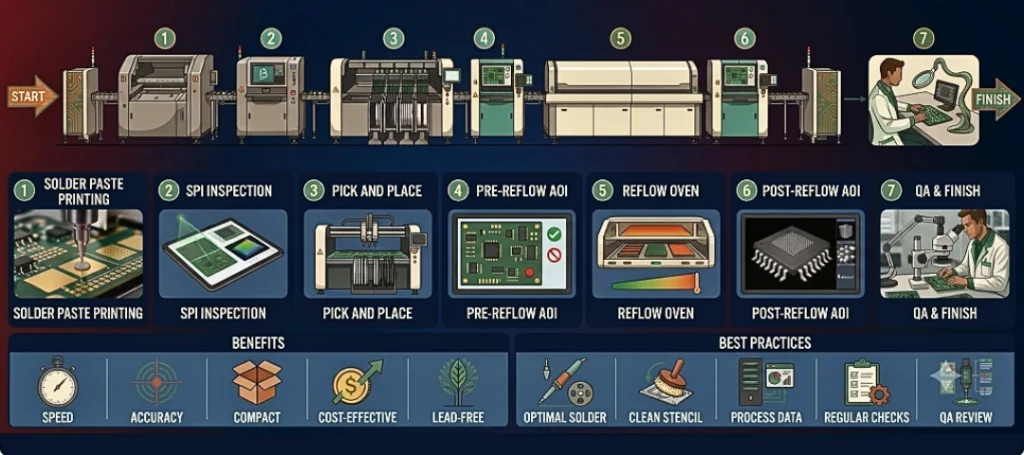
High-level flow diagram of surface mount process
Advantages of Surface Mount Technology
There are various advantages to using this technology, such as the following.
- Cost-Effectiveness: Highly automated manufacturing processes and high-volume runs reduce labor, production time, lead material usage, and component costs while accelerating reliable development.
- Miniaturization: It enables the manufacturing of lightweight, compact, and smaller components that can be used in handheld units, consumer electronics, wearables, and IoT gadgets.
- Flexibility: This technique allows better design flexibility without drilling to accommodate amalgamation of conventional THT and SMT utilized in complex or hybrid schemes.
- HighDensity: A surface mount device can be mounted on the backside of the PCB to increase circuit density and compatibility within tighter spaces, thus leading to feature-rich and smaller electronics, such as those developed through medical device engineering services.
- Reliability: It enhances high-frequency performance (5 GHz) and reliability as components with shorter lead lengths and signal paths are used for less parasitic effects during inductance and capacitance.
- Higher Speed: Manual THT methods are outpaced by automated assembly lines that can produce 1000s of PCBs on a daily basis.
- Resistance: A surface mount device showcases thermal efficiency, durability, low stress and load given their resistance to vibration, fewer leads, and compact attachment.
- Versatility: A wide range of components can be accommodated, from capacitors to fine-pitch processors, rendering SMT as useful and adaptable for diverse electronic applications and systems.
Conclusion
Given the rising demand for PCB and consumer electronics, SMT-based assembly works as a boon for manufacturers. This technology is appropriate for complex applications with the guarantee of preserving quality while it supports the management of fast-moving production lines, as we learnt in this blog about what is surface mount technology. SMT, alongside selective soldering, a part of THT, can improve the first pass yield (FPY) and component positioning.
Although SMT offers superior electrical performance, the initial production costs can be slightly high, such as in FPGA design, and the end solutions might be difficult to repair. Another challenge lies around environmental sustainability issues it poses, as industries are advised to use lead-free solders. Additionally, the Restriction of Hazardous Substances (RoHS) has laid new standards for solder compatibility and other related modifications in SMT procedures. Management and fixing of PCB components may be difficult, while SMT is more preferred for low-stress settings where weaker mechanical bonding is intended.
Manual rework and repair operations are small-size-oriented, and solder connections succumb easily under mechanical pressure and thermal dissipation. SMT is unsuitable for applications that require high-power and large components and needs to undergo complex inspections in case of special feeding plates and absence of lead to hand placements. Tombstoning is an instance when an SMD stands upright on one end because of uneven heating or pad design during reflow soldering, while solder bridging refers to excess solder deposition connecting adjacent pads leading to shorts.
KritiKal assists PCBA manufacturers in overcoming these challenges through best practices that follow industry guidelines for surface mount process, like ISO 9001, IATF 16949 (automotive), AS9100D, ISO 13485 (medical devices), IPC-A-610 Class-II (generalized industries) to Class-III (aerospace and medtech) that define workmanship acceptance levels. We conduct AXI and functional testing procedures for BGAs and other obscured connections within assembled products, especially for medical device testing. We can be your fast-turn SMT assembly partner for implementing digital transformation, developing clean, functional PCBs that surpass evolving challenges in short-run design, validating products with 3D AOI, vapor-phase reflow, and refining prototypes with speed, precision, and quick-turn flexibility.
We offer smart manufacturing solutions, stay up to date with DFM practices, innovations in low-temperature solder alloys, thermal interface material (TIM), high-density substrates, and instigate the use of lightweight, compact, high-performance, fine-pitch, and miniaturized/micro-scale SMDs. We prevent tombstoning by using symmetrical pad sizes and balanced thermal profiles and solder bridging by using precise stencil and maintaining mask clearance of 0.1 mm. We negate the presence of contaminants like dust and chemical residues, and misalignment of components from incorrect pick and placement by continuously calibrating machines and using fiducial marker on the PCB accurately. Please get in touch with us at sales@kritikalsolutions.com to know more about our embedded products, platforms, services, and reduce the time of your ideas taking shape.

Jagpal Singh currently works as a Senior Support Engineer at KritiKal Solutions. He has over 13 years of experience in working on embedded systems, firmware and hardware designing, analog, digital semiconductors, hardware analysis, PCB layout, PIC, ESP32, STM microcontrollers, and more. He is proficiently skilled in problem solving, Embedded C, C++, Python, CSS, HTML, Git, SQL, Arduino, MPLAB, STM, etc. and has helped KritiKal in delivering various projects to some major clients.