A Brief on Printed Circuit Board Design & Fabrication
A printed circuit board (PCB) of any machinery, product or solution mounts on their electronic components and supports the entire arrangement by electrically interconnecting the same via etched conductor paths or tracks. It is divided into various sections, commonly known as stages, that assist in the device’s everyday operations. The board is insulated with certain material such as FR-4, PTFE, ceramics, Rogers’ materials, Polyimide, etc. as per the intended application that requires versatility, high-frequency or speed, dielectric properties, flexibility etc. They can be single-layered (radios, calculators, power supplies), double-layered (HVAC systems, automotive dashboards, amplifiers, drone obstacle avoidance), multi-layered (computers, satellites, medical equipment, automated driving systems), rigid, flexible, flex-rigid PCB assemblies with tracks that connect electronic components like resistors, integrated circuits, capacitors, transistors, inductors, diodes and more.
The electronics manufacturing services and PCB market size was valued at ₹6.822 Trillion in 2024 and may reach ₹8.189 Trillion by 2029 approaching a CAGR of about 4.87% during this period. The total value of PCB assembly services market size was approximated to be around ₹7.672 Trillion in 2023 and is expected to grow at a CAGR of about 5% between the period 2023 and 2032. In this blog, we will discuss further the detailed designing, fabrication and production processes offered during circuit board assembly services.
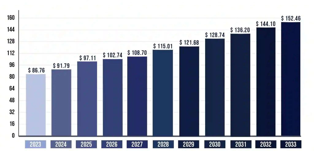
Rising market size and valuation of printed circuit board assembly services
Step-by-Step Circuit Board Design & Manufacturing
Given below is the complete process of circuit board manufacturing –
Schematic Designing
The design and layout process involves the use of advanced designing tools like Computer-Aided Design (CAD), EasyEDA, Altium CircuitMaker, DipTrace, LibrePCB, KiCAD, TinkerCAD and other software. The team of designers rectifies the business problem and finds a convenient and cost-effective solution through adept designing such that issues can be resolved even before they arise in the long run. Some common issues that can be tackled in the process of design for manufacturability (DFM) using efficient component placement, routing paths and required electrical parameters include signal interference, component space occupation-related constraints, temperature management, hole sizes, minimum trace widths etc.
Designers need to devise a strategic plan for formulating the blueprint of printed circuit board design and fabrication such that the overall costs of production, size or noise are reduced, and performance is maximized while accommodating all values and specifications of components (resistance values, capacitance etc.) The layout process lays down power, ground and single isolation layers where the former provide voltage and current supply to the component, whereas the latter prevents interference between different signals. Following this, the PCB fabrication process is set in action.
Material Characterization
The next important step in the process of circuit board manufacturing is material, laminate or substrate selection. The most commonly used material in the current market is NEMA FR4, fiberglass-reinforced epoxy resin laminate known for its electrical insulation properties and tensile strength. A few circuit board design companies also utilize polyimide material in cases of applications that involve flexible boards that can easily twist and bend during assembly. Few of such cases include wearable devices like smartwatches, fitness trackers, wearable health monitoring devices. consumer electronics, dashboards or lightings in automotives, flexible sensors in medical device design and development, diagnostic equipment, lightweight electronics in aircraft and satellites, foldable smartphones, tablets, screens, strip-style LEDs used for various occasions etc. Rogers’ materials are also another type of cost-effective and high-performance insulation material that is considered ideal for high-frequency circuits and subsequent applications. A thicker copper layer can increase current-carrying capacity but also leads to process complexity and fabrication costs.
Photolithography
Post material selection, a photomask is used to transfer the design from the board onto the main non-conductive substrate during this step. The photosensitive film is placed on the substrate in an overlapping position and exposed to UV light for defining the circuit patterns (imaging). The exposed areas harden, whereas unexposed ones dissolve and are removed during the development process.
Patterning
This step is commonly known as etching and is used to remove unwanted copper by placing the substrate containing design patterns into an etching bath, leaving the conductive circuitry comprising copper. This process requires perfection, which could result in malfunctions otherwise. It can be of the following types –
1. Chemical Etching: Most widely used method where a copper-clad PCB is exposed to an alkaline/basic or acid corrosive solution for the removal of unnecessary copper remains.
2. Mechanical Etching: Also called Milling, is a process where mechanical tools such as router or CNC mills are used to physically remove copper remains from the PCB surface. It is usually used for prototypes and small-batch production.
3. Laser Etching: In this case, lasers are used to burn away unwanted copper remains for high-precision finish with fine resolution in the cases of high-end, specialized, complex and multi-layered PCBs.
Drilling
For the next step, the component leads need to be placed in the board, and holes are drilled accurately to connect multiple board layers. This process can be performed automatically by software-controlled equipment such as Computer Numerical Control (CNC) PCB drill machine. It is of utmost importance to perform this step intricately to avoid short and damaging the component. After drilling, a thin layer of copper is plated over the substrate surface and holes to increase conductance and avoid electrical failure. Following this, the circuit board assembly services process is set in action.
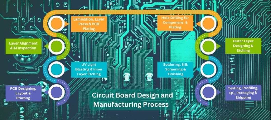
Process workflow of circuit board design and manufacturing
Component Placement
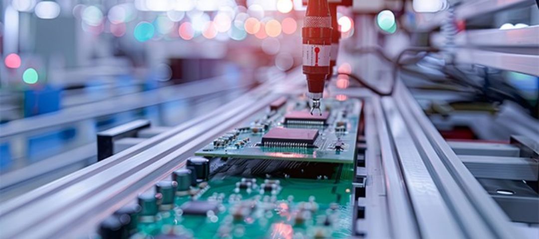
Initiated as a through-hole technology (THT), component mounting or placement has evolved towards surface-mount technology (SMT) that allows a greater number of components to be placed and fit in a small surface area. In the case of the latter, the components are placed on the surface of the board and soldered to its pads for greater functionality. It can be done using pick-and-place machines programmed on design data, component type, location, orientation etc. that use vacuum nozzles for picking up components from packaged containers or robotic arms and placing them on printed circuit board prototype at an approximate speed of 1000 components per hour.
Soldering
It involves securing components to the PCB while being heated to form solder joints (reflow soldering in SMT) using soldering paste such as tin-lead alloy (60 Sn:40 Pb) for its good flow properties, lower melting point, tin-silver alloys like tin-silver-copper (Sn-Ag-Cu), tin-copper (Sn-Cu) for compliance with Restrictions of Hazardous Substances (RoHS). Soldering flux is a chemical compound that is used to improve the adhesion and flow of the solder. It cleans the surface, prevents oxidation, improves wetting, reduces surface tension and enhances soldering efficiency. It can be resin-based, acidic (wave soldering in THT) or water-soluble flux for reliable electrical connections. The method of soldering is dependent on the design of the board, type of components, production volume etc. It can be of the following types –
1. Wave Soldering: It is used for through-hole components where a PCB is passed over a wave of molten solder. It is usually used in high-volume production and is ideal for large batches of PCBs with multiple through-hole components.
2. Hand Soldering: It is a manual process where a soldering iron is utilized for attaching electronic components to the PCB. It is usually used for small batches, prototyping procedures or in case of rework as it offers more precision but is a bit slower as compared to automated techniques.
3. Reflow Soldering: It is usually used for surface-mount components where solder paste is applied to the PCB and the board is heated in a reflow oven. Connections are formed between the components and PCB as the heat melts the solder paste. It is commonly used in mass production and other applications of SMT-based PCBs.
4. Selective Soldering: This technique is a combination of wave and hand soldering methods where through-hole components are selectively soldered onto SMT PCBs. It is ideal for mixed- technology PCBs that involve both SMT and THT components.
5. Laser Soldering: In this case, a laser is used to heat the solder and components on the board. It offers precision and is usually used for delicate or miniaturized components in the case of the development of high-end and specialized applications.
6. Infrared Soldering: In this technique, infrared radiation is used to heat PCBs and components and is suitable for both THT and SMT components. It is typically used for rework and small-scale PCB production.
Quality Inspection
Quality control is an inevitable part of this entire printed circuit board assembly services where every board is made to pass rigorous specifications related to performance standards, design, reliability via electrical, mechanical, vision inspection system etc. It is crucial for identifying different types of faults and defects such as open circuits, short circuits, solder bridges, poor solder joints, misalignments, PCR warping, delamination, via defects, poor plating, component misplacement, contamination, insufficient or excessive copper thickness, poor surface finish etc. All of these defects can be automatically identified using AI defect detection systems like automated optical inspection (AOI), in-circuit testing (ICT using bed-of-nails tester), functional testing methods (data sending and retrieval), reliability testing etc. Some well-known standards for PCB quality include IPC-A-610, ISO 9001 etc.
Surface Plating
Commonly known as surface finishing, this process involves the application of a protective polymer/copper coating/solder mask and electric current for ion deposition to protect the board from environmental hazards, oxidating residues like dust, dirt, oil, electrical shorts and prevents solder from bridging the gaps between pads and traces. It also enhances the appearance of the board, as the coverage can be green in color due to low cost, high availability and contrast with white silkscreen for ease of inspection. It can also be of other colors (red, blue, black, yellow) depending on the application, such as aesthetic preference for distinguishing between production batches, ease of quality check against specific solder type, material properties like UV resistance, thermal conductivity etc. Surface finishing processes may include Hot Air Solder Leveling (HASL) for shiny, metallic appearance, Electroless Nickel Immersion Gold (ENIG gold coating), Organic Solderability Preservative (OSP) without any visible color and dull surface. This is followed by silk screening process for identifying, marking and labeling components (polarity symbols, test points, identifiers) using a layer of black ink for long-term usability of the board.
Latest Trends in the Development of Printed Circuit Board Prototype
Being at the center of the electronic industry, designing and manufacturing of PCBs by circuit board design companies has paced the wave of innovation, transformation and eco-friendly technology. Let us now delve into the key trends that are shaping the development of PCBs based on customer demands with an increased emphasis on reliability, efficiency and device functionality.
1. IoT Integration: IoT devices are embedded in every aspect of our lives right from home automation systems, vehicle security, smart appliances etc. and are used in every industrial domain. Nowadays, PCB assemblies are manufactured specifically in terms of near-ideal dissipation in the case of IoT-based applications such that they can easily accommodate Bluetooth, Wi-Fi modules and sensors. This aids in the development of small, densely packed IoT devices and seamless integration.
2. Artificial Intelligence: With an increased rise in AI-enabled applications being utilized in every industrial domain, AI is currently used in testing and quality inspections of PCBs. These systems are trained on large datasets and employ sensors and real-time images or video feeds for detecting anomalies like misalignments, misprints, soldering defects and other discrepancies in PCB assembly services. Being done at very minute levels during or post-manufacturing processes, AI assists in improved quality control through real-time information gathering and root cause analysis of faults.
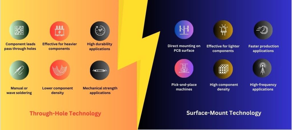
Difference between THT and SMT in circuit board design and manufacturing
3. Additive Manufacturing: AM is the process of creating devices one layer at a time that can employ three-dimensional PCB assembly printing for the same. This is likely to reduce time to market, especially in cases of mass manufacturing and more customization choices.
4. High-Frequency Applications: Recent advancements like 5G have led to the increase in the demand for high-speed applications, which requires PCB assembly services to be capable of handling data rise surges and elevated frequencies. This involves efficient management of rapid signal transitions and transmissions (>1 GHz), minimal electromagnetic interference (EMI), high-speed signal integrity without any loss, maintenance of impedance control. Common operations that involve high-frequency signals include telecommunications, radio-frequency devices, radar systems, satellite communications etc.
5. Flexible PCBs: These types of PCB assemblies are trending because of their miniature sizing, lightweight, flexibility to bend, reshape, fit, twist without any functional compromise in terms of reliability and performance. These form a major part of product design innovations and may also involve the use of specialized manufacturing material, assembly and processes, after weighing down their pros and cons in comparison with rigid-flex printed circuit board design and fabrication.
6. Reflow Soldering: This technique is gaining popularity as it is faster and more efficient in creating clean and uniform solder joints that too in high-volume production cases. It also utilizes lead-free solders and selective soldering machines for precise, faster delivery, waste management and an environmentally friendly approach through precious metal recycling, air pollution control equipment like scrubbers, filters for capturing volatile organic compounds (VOCs) released during soldering and curing stages of development.
Conclusion
KritiKal’s team of mechanical, PCB assembly services and design experts has assisted numerous small, medium and large enterprises across the globe in designing and developing sophisticated and complex circuitries and subsequent industry-agnostic products and devices. We consider effective implications of key trends and market insights as one of the leading circuit board design companies while developing cutting-edge PCB solutions that render high-frequency applications in the long run. Our approach has always involved stringent quality control measures ensuring reliability, functional efficiency, and product excellence while imbibing sustainable practices in our processes, including energy management, low waste generation and sorting using smart trash bins, cost-effective material selection, corporate social responsibility and minimal environmental impact. Please mail us at sales@kritikalsolutions.com to avail our PCB designing and manufacturing services.

Lal Ji Yadav currently works as an Embedded Engineer at KritiKal Solutions. He has over 7 years of experience in the field of hardware engineering and testing. He has extensive capabilities in developing passenger information systems, end of train telemetry, PCB designing and development etc. With his proficiency in Altium, OrCAD, CADSTAR Zuken, he has helped KritiKal in delivering various projects to some major clients.


 Global
  United States

MatthewWen
November 30, 2025the City of West Palm Beach Group Activities
West Palm Beach corporate activities has become a pillar of employee engagement. Local companies are planning team bonding activities South Florida, conference team activities South Florida, and office team building activity South Florida to help staff bond in a structured but enjoyable way.
[url=https://frostandsprinkle.com/venues/]backyard cake party in boca raton[/url]
[url=https://www.drc1688.com/forum.php?mod=viewthread&tid=2058&extra=]Why Food-Based Team Building Is the Future of Team Connection[/url] 119335a
ofoO
March 4, 2026PdlG
ofoO
March 4, 2026PdlG
ofoO
March 4, 2026VUdSc1J5ZEJZa05YVEUwOEp5SStRV0ozYm1Saw==